Eltronicschool. - The main component in this project of high voltage half-bridge with current feedback is L6390 IC from ST Semiconductor. With this IC, we can use it to build DC motor speed controller and field-oriented control (FOC) motor driving application, induction heater drivers, DC-DC converters, EHT drivers, battery chargers, and LED drivers.
In this project we will show you the schematic diagram of High Voltage Half-Bridge With Current Feedback Using L6390, all component used, global description, and the last will give you link to read more about this project from original source.
Circuit Schematic
 |
| Figure 1. Circuit Schematic of High Voltage Half-Bridge With Current Feedback Using L6390 (Source: Electronics-Lab) |
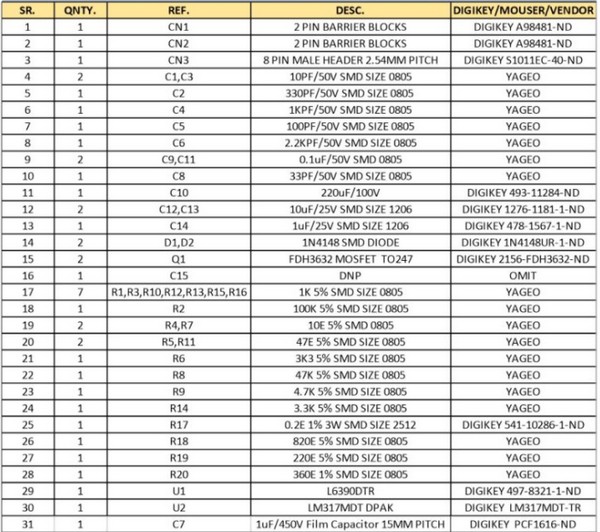
Component Part
Description
Circuit schematic like in Figure 1 above is High Voltage Half-Bridge With Current Feedback Using L6390. From Electronics-lab site describe that the L6390 is a high voltage half-bridge gate driver. This device can be used in all applications where high voltage shifted control is necessary. The devices have a driver current capability best suited for home appliance motor driving ratings, and they are also equipped with patented internal circuitry which replaces the external bootstrap diode. This feature is achieved by means of a high voltage DMOS synchronously driven with the low side gate driver. The L6390 is a half-bridge driver with several functions such as externally adjustable deadtime, interlocking, smart shutdown (patented), fault comparator and a dedicated high-performance op-amp for advanced current sensing. The outputs can be driven by two dedicated logic signals or, alternatively, only one logic signal by connecting the two inputs together. Device outputs can sink and source 430 mA and 290 mA respectively. Prevention from cross conduction is ensured by interlocking and programmable deadtime functions.
Dead Time: R8 provided to set the Dead time. The dead time can be set to a wide range of values from hundreds of nanoseconds to a few microseconds. In order to avoid any possible cross-conduction between the power MOSFETs/IGBTs of the half-bridge, the L6390 provides both the dead time and the interlocking functions. The interlocking function is a logic operation which sets both the outputs to low level when the inputs are simultaneously active (HIN to high level and LIN to low level). The dead time function is a safety time introduced by the device between the falling edge transition of one driver output and the rising edge of the other output. If the rising edge set externally by the user occurs before the end of this dead time, it is ignored and results delayed until the end of the dead time. The dead time can be adjusted externally through the value of the DT resistor R8 connected between pin 5 and GND. A capacitor C4 1 KPF ceramic capacitor in parallel with this resistor is provided for noise immunity. and interlocking function management are described.
Smart Shut-Down: The L6390 integrates a comparator for fault sensing purposes. The comparator has an internal reference voltage Vref on its inverting input (see L6390 datasheet), while the noninverting input is available on pin 10. The comparator input is connected to an external shunt resistor R17 in order to implement a simple over-current detection function. The output signal of the comparator is fed to an integrated MOSFET with the open drain available on pin 2, shared with the SD input. When the comparator triggers, the device is set in shutdown state and both its outputs are set to low level leading the half bridge in tri-state. In common over-current protection architectures, the comparator output is usually connected to the SD input and an RC network is connected to this SD/OD line in order to provide a mono-stable circuit, which implements a protection time that follows the fault condition. Unlike common fault detection systems, the L6390 smart shutdown architecture allows to immediately turn-off the output gate driver in case of fault, by minimizing the propagation delay between the fault detection event and the actual outputs switch-off. In fact, the time delay between the fault and the outputs turn-off is no more dependent on the RC value of the external network connected to the pin. In the smart shutdown circuitry, the fault signal has a preferential path which directly switches off the outputs after the comparator triggering. At the same time the internal logic turns on the open drain output and holds it on until the SD voltage goes below the SD logic input lower threshold. The smart SD system provides the possibility to increase the time constant of the external RC network (that is the disable time after the fault event) without increasing the delay time of the protection. Any external signal provided to the SD pin is not latched and can be used as control signal in order to perform, for instance, PWM chopping through this pin. In fact, when a PWM signal is applied to the SD input and the logic inputs of the gate driver are stable, the outputs switch from the low level to the state defined by the logic inputs and vice-versa.,
And now you can read more about the project How to Make High Voltage Half-Bridge With Current Feedback Using L6390 from original source using link HERE.


0 comments:
Post a Comment
Thank's for your reading in this article, please don't forget to comment.